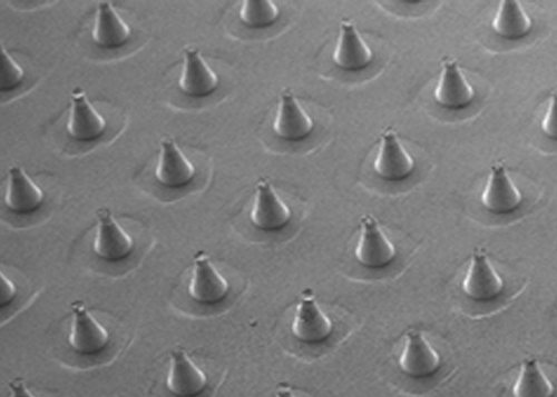
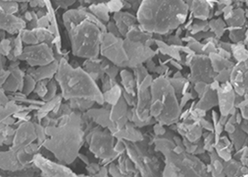
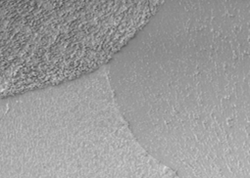
The Scanning Electron Microscope (SEM) allows visualization of surface features of a solid sample by scanning through an electron beam. SEM has better resolution capability and depth of field than a light microscope. Therefore, good quality three-dimensional like images are obtained.
In advanced JEOL JSM IT 200 SEM machine, magnification ranges from 10X to 3, 00,000X and resolution of about 10 nm. The surface view and cross-sectional view of the sample can be easily observed. In addition, the elemental composition and mapping of any solid material can be found out by EDX analysis.
Samples from textile, pharmaceutical, ceramic, polymer, metal and other allied industries can be tested on this SEM machine.
Samples which can be Analyzed
A wide range of materials whose morphology can be routinely analyzed include:
Metals, Glass, Ceramics and Polymers
Semiconductors
Plastics
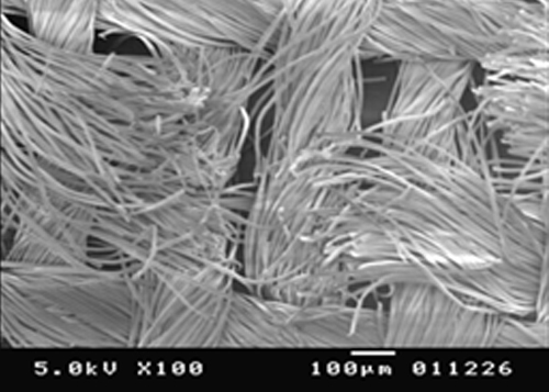
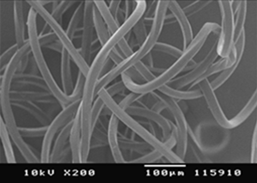
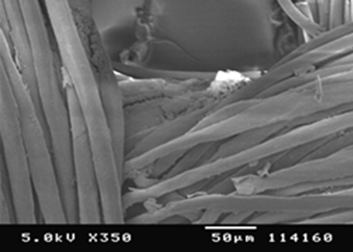
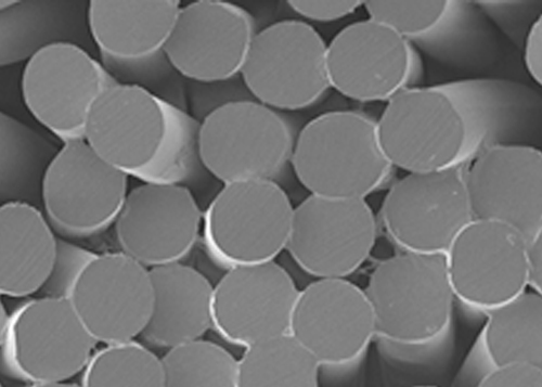
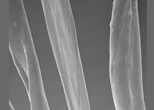
Fibers (Textile, Glass, Asbestos, Natural)
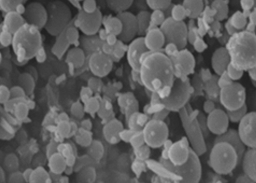
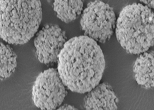
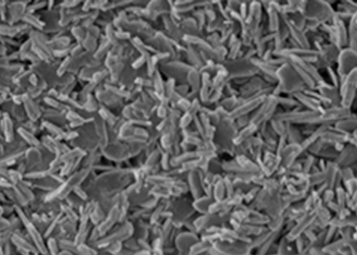
Powders and Dust
Pharmaceutical powder, pellets, capsules
Samples can be analyzed provided these are vacuum compatible and not damaged by heat produced by electron beams.
Range of Applications
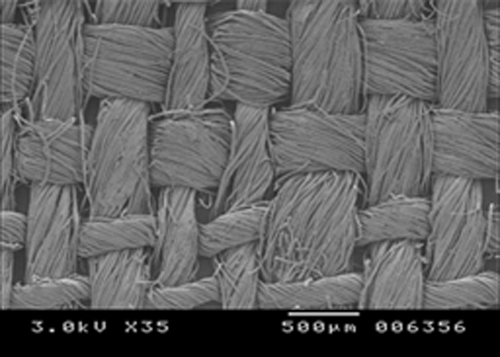
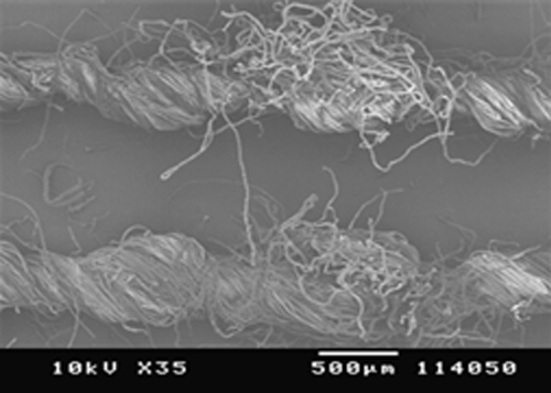
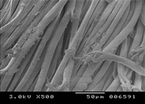
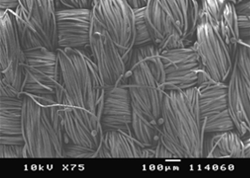
Examination of surface morphology
Defect analysis of textile materials
Cross-section and longitudinal imaging of filaments/yarns
SEM provides micrographs with scales which can be used to get some quantitative information like the distance between two points on the micrograph. It can also be used to find the pore size, shape of a feature. But, it does not provide topographical height information like AFM does.
